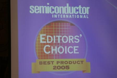
GN's AFM Guided Nanomachining Invention receives an award as the Best Product of the Year from the semicondcutor community and Semiconductor International!
05/18/2005
Robert Monteleone Senior Analyst with Wall Street Reporter interviewed the GN CEO Mr. Vic Kley. Click here to listen.
03/07/2003
FOR IMMEDIATE RELEASE
CONTACT:
General Nanotechnology
info@gennano.com
www.gennano.com
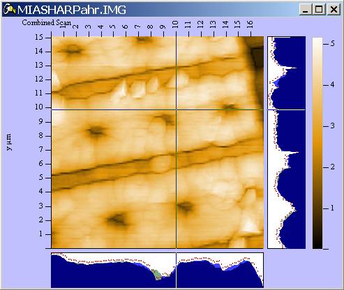
General Nanotechnology (GN) announces Probe Version 3; for visualizing, measuring, enhancing, analyzing and annotating of 3D images from any instrument.
The first low cost means for pointing and interacting with 3D surfaces.
Berkeley, CA. March 7, 2003 -General Nanotechnology announced today Probe Version 3, its latest visualization software with the first friendly natural solution for directly interacting with 3D surfaces from a normal 2D display. GN has patented and produced the embedded cursor allowing users to finally point to any part of a 3D surface without the need for cumbersome goggles, special screens or unwieldy and expensive 3D pointing devices.
Although the technology supports any cursor shape, GN
has chosen a Maltese cross with a special adaptive outline which is visible
on any background regardless of brightness or shadow. Using any standard
mouse the user can effortlessly slide the cursor over any complex surface
to reach any point. Embedded in the surface the cursor is visible as the
surface is rotated and moved to new viewpoints. Measurement cursors and
flags also can be seen on the 3D surface as the user makes a virtual cut
to measure the surface along the cutting plane.
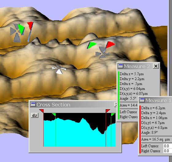
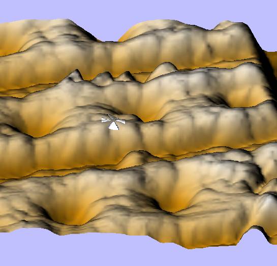
Probe offers many other unique software tools for measuring, enhancing, analyzing and annotating of 3D images. With Probe 3, it is now possible to open any file in 2 dimensions, and show the X and Y cross sections in 3D orthogonal views.
For additional information about General
Nanotechnology and its products (Probe™
Visualization Software and nanotool™
V, its breakthrough series of unique capability NEMS
SPM tips), contact Michelle Conci at 650-458-8522 or email michelle@gennano.com
or visit the website at www.gennano.com.
nanotool is a trademark of General Nanotechnology, and all other trademarks
are property of their respective owners.
03/03/2003
FOR IMMEDIATE RELEASE
CONTACT:
info@gennano.com
www.gennano.com
General Nanotechnology expands the revolutionary Nanotool V Series of active cantilevers in response to customer demand, creating additional characteristics to support for the nanotech, biotech and semiconductor industries.
Berkeley, CA. March 3, 2003-- General Nanotechnology, the creator of AFM Guided Nanomachining, today announces the availability of an entire family of function specific diamond tipped active cantilevers nanotool™ V Series, for research and industrial applications using Scanning Probe Microscopy (SPM) to make or measure things at scales as small as a few atoms. The first significant advance in basic SPM cantilever design in almost 20 years, the nanotool V permits new modes of nanomanipulation and nanomachining, for many applications, and extends the benefits of SPM to process applications where wear and other limitations closed the door to commercial applications.
"The nanotool V Series was first introduced last December at the Integrated Nano Systems show in Berkeley. Since then, we have sampled specific variations to interested parties, and based on that demand, are making them commercially available", says Vic Kley, CEO of GN.
As enabling components for new Nanotechnology applications, the nanotool
V series consists of a Digital Instruments footprint MEMS platform capable
of many new functions and features including a thermal force generator
that enables clamping of the tip platform for full immobilization of the
tip, and to provide use specific higher spring constants to the mechanical
action of the tip and primary cantilever (10s to thousands of Newton/meters).
Precisely oriented and controlled single crystal diamonds provide extreme
durability, while software and hardware controlled spring constants provide
High Q scans and high force probing or nanomachining.
Save this for a new release we have not announced it as available. The
Series V MEMS Cantilevers provide the first true multi-mode SPM operation
with out loss of sample position for mixed AFM/STM/Conductivity Probing
and nanomanipulation.
For additional information about General Nanotechnology or the nanotool
V series, contact info@gennano.com
or visit the website at www.gennano.com.
General Nanotechnology (GN) is a California Limited Liability Company
(LLC), that develops hardware and software for advanced capabilities in
imaging, nano-manipulation, nano-fabrication, nano-spectro-photometry,
near field optical probes below the aperture (50nm) limit, and diamond
and other nanotools™ tips and parts.
Its principal operational location is in Berkeley, California. GN has
partnered with the Lawrence Berkeley National Labs in a three-year nanodevices
and tips development program. GN's licensee is the manufacturer of the worlds first commercial
SPM based nanomachining system.The licensee uses GN's groundbreaking
inventions in SPM nanomachining and control software.
nanotool is a trademark of General Nanotechnology, and all other trademarks
are property of their respective owners.
01/23/2003
FOR IMMEDIATE RELEASECONTACT: info@gennano.com www.gennano.com
Vic Kley, CEO of General Nanotechnology (GN) announces he will address the first World Nanotechnology Summit
CEO and founder to talk about tools for directed nanotechnology and present GN's spin-out strategy
Berkeley, CA. January 23, 2003 -General Nanotechnology announced today that Vic Kley, CEO and founder, will address the first World Nanotechnology Summit in New York, April 7 - 10. Mr. Kley will speak in the morning session as an expert on the topic of the creation and exploitation of nanotechniques, and in the afternoon sessions as a presenting company; speaking about GN as an R&D group and its spin-out strategy for companies that can take advantage of GN's basic inventions for the biotechnology, metrology and other areas for nano-fabrication and nano-manipulation.
"The World Nanotechnology Summit is designed to bring together the world's most pioneering individuals and best-of-class nanotechnology ventures that define the current nanotechnology landscape," said Mr. Ole Nielsen, President and CEO of conference organizers Emerging Technologies. "The pace of advancement in nanotechnology research is dictated by the availability of state-of-the-art tools and instruments such as
Vic Kley, CEO of General Nanotechnology (GN) announces he will address the first World Nanotechnology Summit
those developed by General Nanotechnology, so we are delighted to have Vic Kley, who is widely respected as a pioneer in the nanotechnology tools and instruments market, share his extensive experience with our audience."
The World Nanotechnology Summit (WNS2003) is a milestone nanotechnology event that, for the very first time, brings together leading executives, investors and advisors from around the world to discuss the leading edge of nanotechnology from a commercial, rather scientific, perspective.
Vic Kley founded General Nanotechnology (GN) in 1992, and GN is the creator of Atomic Force Microscopy Guided Nanomachining (AGN); a technique now commercially used by Semiconductor manufacturers in the Silicon Valley and abroad to make repairs on difficult, next generation semiconductor production tools called MASKs. GN's successful spin out for Mask Repair Tools, our licensee, has demonstrated the capability to repair the next three generations of Masks. GN also developed visualization and control software for SPM, Confocal and standard optical systems, which are presently used in products made or sold by IBM, KLA/Tencor, Veeco, Nikon, FEI and our licensee.
For additional information about General Nanotechnology and its products (ProbeT Visualization Software and nanotoolT V, its breakthrough series of unique capability NEMS SPM tips), contact info@gennano.com or visit the website at www.gennano.com. For additional information about WNS2003, visit http://www.nanotechsummit.com
nanotool is a
trademark of General Nanotechnology, and all other trademarks are property
of their respective owners.
09/19/2002
FOR IMMEDIATE RELEASECONTACT: mailto:info@gennano.com www.gennano.com
GN Introduces a New Paradigm for SPM, NanoManipulation, Nano electrical
and chemical Probing and Nanomachining
Berkeley, CA. September 19, 2002 -- General Nanotechnology, the creator
of AFM Guided Nanomachining, today announces the availability of the nanotoolT
V, a series of active cantilevers with diamond and conductive diamond
tips. The first significant advance in basic SPM cantilever design in
almost 20 years, the nanotool V permits new modes of nanomanipulation
and nanomachining, for many applications including industrial and biotechnology
industries, and extends the benefits of SPM to process applications where
wear and other limitations closed the door to commercial applications.
GN expects the nanotool V and its descendents to be enabling components
for new Nanotechnology Companies and Industries. The nanotool V debuts
today at the Integrated Nano Systems show in Berkeley, with specific styles
to be sampled to qualified researchers and companies.
The basic nanotool V series consists of a Digital Instruments footprint
MEMS platform capable of many new functions and features including a thermal
force generator
GN Introduces a New Paradigm for SPM
that enables clamping of the tip platform for full immobilization of the
tip, or to provide higher spring constant to the mechanical action of
the tip and primary cantilever. Precisely oriented and controlled single
crystal diamonds provide extreme durability, while software and hardware
controlled spring constants provide High Q scans and high force probing
or nanomachining.
The design includes an optional subsystem for delivery of gases, fluids
or vacuum to a 50 by 25 micron volume at the base of the SPM tip. Permitting,
among other things, liquids operation without a liquid chamber or petri
dish for biotechnical applications. Many more functions are incorporated
into the design and may be announced over the next year as they reach
production readiness.
For additional information about General Nanotechnology or the nanotool
V, contact Michelle Conci at 650-458-8522 or michelle@gennano.com
or visit the website at www.gennano.com.
General Nanotechnology (GN) is a California Limited Liability Company
(LLC), that develops hardware and software for advanced capabilities in
imaging, nano-manipulation, nano-fabrication, nano-spectro-photometry,
near field optical probes below the aperture (50nm) limit, and diamond
and other nanotoolsT tips and parts. Its principal operational location
is in Berkeley, California. GN has partnered with the Lawrence Berkeley
National Labs in a three year nanodevices and tips development program. Our licensee is
the
manufacturer of the worlds first commercial SPM based nanomachining systemn. Our licensee is also a licensee of GN's ground-breaking inventions in SPM nanomachining
and control software. nanotool is a trademark of General Nanotechnology,
and all other trademarks are property of their respective owners.
General Nanotechnology (GN) developed the enabling technology behind the first commercial nano-machining system using shaped tools. This system identifies and repairs small defects and anomalies in semiconductor masks.
GN's technology enables mask repair capability on leading edge alternating and attenuated phase shift masks.
This new nano-machining mask repair tool provides mask makers with the ability to remove defects in quartz and molybdenum silicide masks to 130 nanometer mask specification rules. Key capabilities delivered to date are edge placement of 25 nanometers and trench depth controls less than 10 nanometers, with excellent control of the optical transmission characteristics of the repaired region.
The ability to nano-machine defects in quartz and to work inside 500 nanometer lines/spaces and 250 nanometer trenches removes a critical roadblock in the development of production processes development for leading edge phase shift masks.
The system has been designed and built to support 130 nanometer design rule requirements and will be extendable through system upgrades to 100 nanometer rules by mid year 2002.
GN's future
plans are to partner with existing firms or to spin out operations to
exploit its new techniques for Biological, Medical, Material Science,
Chemical Engineering and other process, product and analytical fields.
GN decided
in 1996 to spin out its first major product for Mask and Semiconductor
Repair using a patented special SPM design and its unique, proprietary
nanoscale diamond tool technology as a separate company.
Focusing most of our efforts in the intervening period on assisting a
successful launch of our licensee, we are
especially proud to announce our licensee's first major multi-million
dollar product sale to Infineon in Munich, Germany.
Beginning in 2002 GN will look to exploit this unique technology for Biological, Biomedical, Chemical Engineering and Optical applications through new alliances and a new spin-out nanotoolsT tips (a California Limited Liability Company).
Vic Kley
President
![]()
![]()
ABOUT | PROBE 3D | SMARTFOCUS | GALLERY | DEMO | CONTACT | HOME
COPYRIGHT
2001- GENERAL NANOTECHNOLOGY. LLC. ALL RIGHTS RESERVED.